To some degree, all electric circuits interact with one another. Typically, this is an undesired effect – why do you think consumer electronics have to go through such stringent FCC compliance testing? This interaction may be at a minuscule level that will go completely undetected or it may disrupt the operation of your circuit. One mechanism of interaction between circuits is through mutual capacitance.
Mutual capacitance is the proportionality factor by which a...
Read More
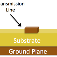
The importance of PCB interconnect techniques increases with frequency of operation. At higher frequencies, transmission line wiring provides superior performance by minimizing crosstalk, signal distortion and radiation (as compared to ordinary point-to-point wiring). When implementing transmission lines on a PCB, there are two options: microstrip and stripline.
Microstrip
A microstrip transmission line consists of a copper trace separated from a ground plane by an insulating...
Read More
In our PCB construction article, we outlined the fabrication process and the basic building block from which custom PCBs are most commonly created – 2 layers of conductor separated by a fixed-width substrate. In this article, we’ll dig deeper into the properties of the constituent parts of this building block.
Conductor
Unless you’re making an exotic PCB, your conducting material will be copper. When fabricating a copper conductor PCB, the only real flexibility you...
Read More
Building Blocks
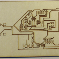
It may be difficult to fathom but each PCB layer is created one at a time. These individual pieces are then bonded together to form your final PCB stackup. The most common PCB building block is 2-layer stock material. This material is two copper sheets laminated to either side of a fixed thickness substrate. This may sound complicated, but it’s just a fancy way of saying: a nonconductive material sandwiched between two pieces of copper.
Example
The...
Read More
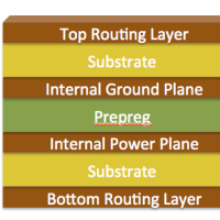
Printed circuit board (PCB) stackup describes the basic construction of a PCB. Specifically, the stackup defines the total number of PCB layers and the type of each of these layers. While the order of some layers are obvious from their names, such as Top Overlay, Bottom Solder Mask, etc., the location of other layers is not so obvious, e.g., Internal Ground Plane 1 or Internal Routing Layer 3. Without a clear description of the PCB stackup, the specific location of these internal layers...
Read More
Printed circuit boards have many different types of layers. To the uninitiated these layer types can be quite confusing, but once you have a basic understanding, you’ll see that it is all quite simple.
Common PCB Layer Types
Mechanical Layer
Keep Out Layer
Routing Layers
Ground Planes & Power Planes
Split Planes
Overlay / Silkscreen Layers
Solder Mask Layers
Solder Paste Layers
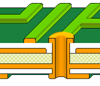
The figure below depicts a three dimensional view of a 4-layer PCB that has two routing...
Read More


Recent Comments